Cryo-SNOM studies of LAO-STO interface
Oxide interfaces have attracted much attention after the discovery of a conducting 2D electron gas, 2DEG, (or 2D electron system, 2DES), with a high carrier density of ~5∙1013 cm-2 in between the two large-bandgap insulators SrTiO3 and LaAlO3 [1] (Fig. 1a). Interestingly, the 2DEG is formed only at and above a critical thickness of LAO of 4 unit cells [2]. Remarkable features of this system are a high electron mobility, magnetism, spin-orbit interaction and even superconductivity [3]. The 2D carrier density and the mobility are temperature dependent, the latter changing by two orders of magnitude between the ambient- and low-temperature. The residual resistivity at low temperature and the superconducting transition temperature can be controlled by the gate voltage [4], which makes this system interesting for oxide electronics.
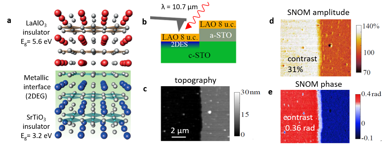
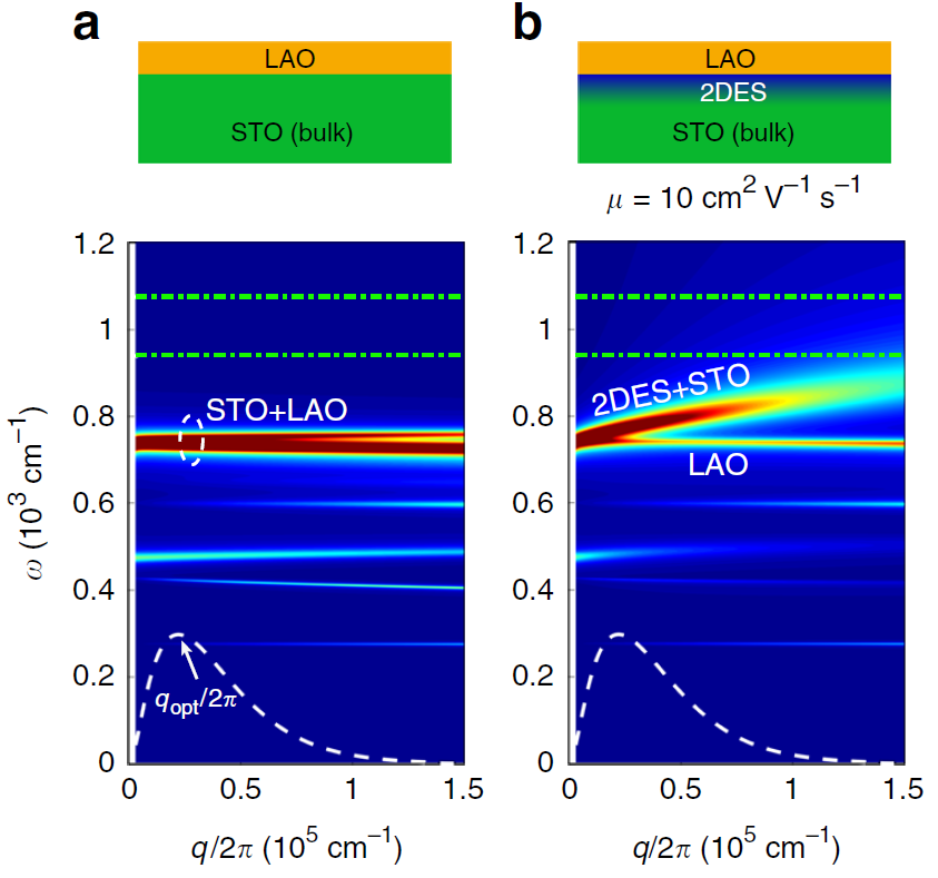
Probing the local transport properties of two-dimensional electron gases confined at buried interfaces requires a non-invasive technique with a high spatial resolution operating in a broad temperature range. In Ref.[5], we used our cryo-SNOM to study the conducting SrTiO3/LaAlO3 interface from room temperature down to 6 K. We showed that the near-field optical signal, in particular the SNOM phase, is highly sensitive to the presence of the 2DEG (Fig.1b-e) and strongly dependent on its transport properties. Using modeling, we established that such sensitivity originates from the interaction of the AFM tip with coupled plasmon–phonon modes where the phonon-polaritons (PhPs) in STO are hybridized with plasmon-polaritons (PPs) in the 2DEG, with the dispersion shown in Fig.2.
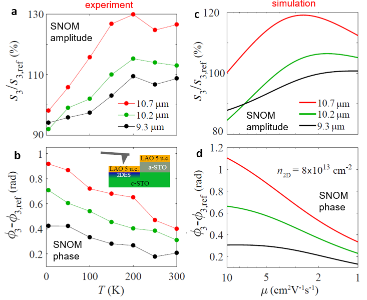
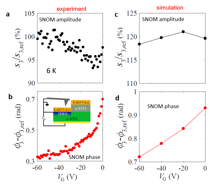
The model explains the observed strong changes in the optical signal with the variation of the 2DES transport properties induced by cooling (Fig.3) and by electrostatic gating (Fig. 4).
To probe the spatial resolution of the technique, we imaged conducting nano-channels written in insulating heterostructures with a voltage-biased tip of an atomic force microscope (Fig.5). One can see that the written wires are clearly seen in the amplitude and especially in the phase. At the same time they are indistinguishable in topography.
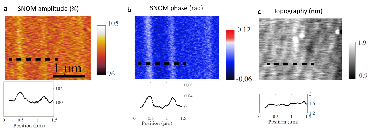
The ability to visualize buried nanoscale conducting structures shows clearly the usefulness of this technique for the development of oxide interface based electronics. It complements other invasive and non-invasive techniques by offering nanoscale information about infrared optical response. We foresee that the use of this local optical probe, in combination with cryogenic performance and electrostatic gating, will provide important information on the possible phase separation and charge inhomogeneities due to ferroelectric domain walls, metal-insulator transitions and other emergent phenomena in a large family of 2D oxide interfaces.
References:
[1] A. Ohtomo and H.Y. Hwang, Nature 427 423 (2004).
[2] S. Thiel, G. Hammerl, A. Schmehl, C.W. Schneider, J. Mannhart, Science 313, 1942 (2006).